Next Generation Silicon Photonic Optical Network
Product News Tuesday, November 29, 2016: FLIR Systems
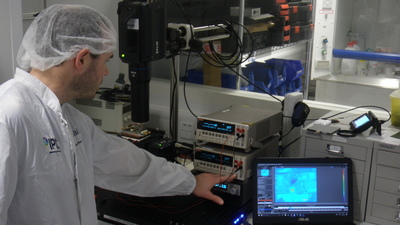
FLIR Systems X6540sc thermal imaging camera is being used by the Photonics Packaging Group at the Tyndall National Institute (Cork, Ireland) as part of a thermal microscope system to image the silicon photonic optical network unit (ONU) for next generation passive optical networks (NG-PONs) developed in the European FP7-Project "FABULOUS”.
Researchers at Tyndall are developing a next generation passive optical network (PON) demonstration module for high-speed fibre-to-home internet connectivity. At the heart of the PON is a silicon photonic integrated circuit (Si-PIC) that receives information on an incoming optical-signal (downloading), before reflecting the optical signal back, after encoding extra information (uploading). In this device an electronic integrated circuit (EIC) is bonded to the top of the Si-PIC, to precisely distribute the electronic timing-signals that are needed to drive the optical modulator in the photonic-chip.
Joule-heating from these high-frequency timing-signals causes an increase in the temperature of the EIC and Si-PIC, which can have a significant impact on the performance and reliability of the photonic-chip. Using the FLIR X6540sc thermal imaging camera has allowed Tyndall researchers to simultaneously measure the EIC and Si-PIC temperatures in different operating modes, so that they can chose the most efficient way to thermally stabilize the photonic-chip. Dr Lee Carroll, research manager at the Photonics Packaging Group at Tyndall commented "The last decade has seen the emergence of silicon photonics as a vehicle for next-generation information communication technology applications. The need for high-performance optoelectronic devices is driven by an ever-increasing demand for higher bandwidth in data and telecom networks. One practical solution for the efficient distribution of high-speed electrical modulation onto the photonic platform is the face-to-face stacking (3D-integration) of a driver electronic integrated circuit on top of a silicon photonic integrated circuit (Si-PIC)".
Dr Kamil Gradkowski, another researcher at the Packaging Group continued "The thermal behaviour of a packaged Si-PIC can impact the performance, stability, and life-time of the device. We use a combination of thermal modelling and temperature measurements to characterize the thermal behaviour of a packaged PIC. Being able to conduct high resolution (640 x 512 pixel) thermal measurements at high frame rates (100 Hz) using the FLIR X6540sc camera has shown that thermal management of the photonic module accounts for approximately 30% of the overall power budget, and so is a significant factor in the overall operational cost. We aim to use the camera to evaluate future packaging designs that are better optimized for cooling".
The X6540sc thermal imaging camera from FLIR Systems provides ultra-fast frame-rate acquisition for scientific and research applications involving dynamic thermal events. The device features a 640 × 512 digital InSb detector with spectral sensitivity from 1.5 to 5.5 µm and an f/3 aperture. It provides images up to 125 Hz in full frame and up to 4011 Hz in a 64 × 8 sub windowing mode. Features on this research grade camera include high thermal sensitivity, snapshot imagery, a motorised spectral filter wheel and a detachable touch-screen LCD. The camera connects to the company’s ResearchIR Max R&D software for thermal imaging data acquisition, analysis and reporting. The X6540sc can be temperature-calibrated up to 300 °C, or up to 3000 °C with spectral and/or neutral density filters, and it provides measurement accuracy of ±1 °C for standard configurations. For further information on the X6540sc thermal imaging camera please contact FLIR Systems at research@flir.com or +32-3665-5100. For further information on the work being undertaken by the Photonics Packaging Group at the Tyndall National Institute please contact lee.carroll@tyndall.ie.
The Tyndall National Institute (www.tyndall.ie) is a leading European research centre in integrated Information and Communications Technology hardware and systems that specialises in both electronics and photonics – materials, devices, circuits and systems. The Photonics Packaging Group at Tyndall is involved in a wide range of international academic and industry projects, with a special focus on packaging and integration for silicon photonics. The group has extensive design, packaging, testing and reliability-testing facilities. Key capabilities include; optical, mechanical, thermal and electrical design, fibre-coupling (single-fibre and fibre arrays), flip-chip integration of both photonic and electronic devices, jetting of micro solder spheres, active alignment of micro-optical benches, high-speed testing, reliability-lifetime-failure analysis of packaged photonics devices.
